
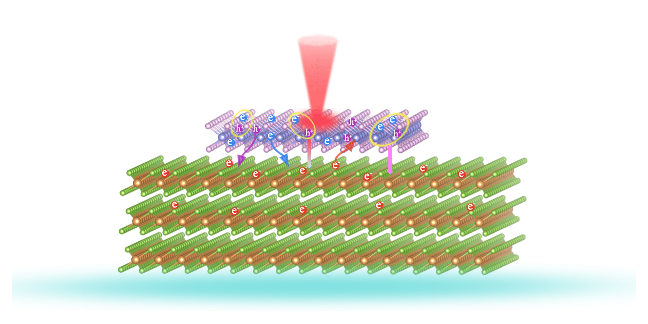
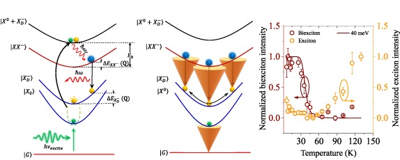
 The monolayers of semiconducting transition metal dichalcogenides host strongly bound excitonic complexes and are an excellent platform for exploring many-body physics. Here we demonstrate a controlled kinetic manipulation of the five-particle excitonic complex, the charged biexciton, through a systematic dependence of the biexciton peak on excitation power, gate voltage, and temperature using steady-state and time-resolved photoluminescence. With the help of a combination of the experimental data and a rate equation model, we argue that the binding energy of the charged biexciton is less than the spectral separation of its peak from the neutral exciton. We also note that while the momentum-direct radiative recombination of the neutral exciton is restricted within the light cone, such restriction is relaxed for a charged biexciton recombination due to the presence of near-parallel excited and final states in the momentum space.
More details: 2D Materials, 9 015023, 2021.
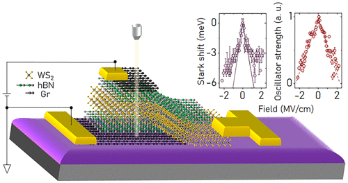
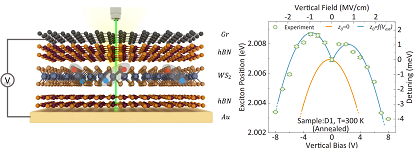 Monolayer transition-metal dichalcogenide (TMDC) semiconductors host strongly bound two-dimensional excitonic complexes, and form an excellent platform for probing many-body physics through manipulation of Coulomb interaction. The quantum confined Stark effect is one of the routes to dynamically tune the emission line of these excitonic complexes. In this paper, using a high-quality graphene/hexagonal boron nitride (hBN)/WS2/hBN/Au vertical heterojunction, we demonstrate an out-of-plane electric-field driven change in the sign of the Stark shift from blue to red for four different excitonic species, namely, the neutral exciton, the charged exciton (trion), the charged biexciton, and the defect-bound exciton. Such universal nonmonotonic Stark shift with electric field arises from a competition between the conventional quantum confined Stark effect driven redshift and a suppressed binding-energy driven anomalous blueshift of the emission lines, with the latter dominating in the low-field regime. We also find that the encapsulating environment of the monolayer TMDC plays an important role in wave-function spreading, and hence in determining the magnitude of the blue Stark shift. The results for neutral and charged excitonic species are in excellent agreement with calculations from the Bethe-Salpeter equation that use a seven-band per spin tight-binding Hamiltonian. The findings have important implications in probing many-body interaction in two dimensions as well as in developing layered semiconductor based tunable optoelectronic devices.
More details: Physical Review B, 103, 075430, 2021.
 In the 1H monolayer transition metal dichalcogenide, the inversion symmetry is broken, while the reflection symmetry is maintained. On the other hand, in the bilayer, the inversion symmetry is restored, but the reflection symmetry is broken. As a consequence of these contrasting symmetries, here we show that bilayer WS2 exhibits a quantum confined Stark effect (QCSE) that is linear with the applied out-of-plane electric field, in contrast to a quadratic one for a monolayer. The interplay between the unique layer degree of freedom in the bilayer and the field driven partial interconversion between intralayer and interlayer excitons generates a giant tunability of the exciton oscillator strength. This makes bilayer WS2 a promising candidate for an atomically thin, tunable electro-absorption modulator at the exciton resonance, particularly when stacked on top of a graphene layer that provides an ultrafast nonradiative relaxation channel. By tweaking the biasing configuration, we further show that the excitonic response can be largely tuned through electrostatic doping, by efficiently transferring the oscillator strength from neutral to charged exciton. The findings are prospective toward highly tunable, atomically thin, compact, and light, on chip, reconfigurable components for next generation optoelectronics.
More details: ACS Photonics, 7, 12, 3386–3393, 2020.
In the 1H monolayer transition metal dichalcogenide, the inversion symmetry is broken, while the reflection symmetry is maintained. On the other hand, in the bilayer, the inversion symmetry is restored, but the reflection symmetry is broken. As a consequence of these contrasting symmetries, here we show that bilayer WS2 exhibits a quantum confined Stark effect (QCSE) that is linear with the applied out-of-plane electric field, in contrast to a quadratic one for a monolayer. The interplay between the unique layer degree of freedom in the bilayer and the field driven partial interconversion between intralayer and interlayer excitons generates a giant tunability of the exciton oscillator strength. This makes bilayer WS2 a promising candidate for an atomically thin, tunable electro-absorption modulator at the exciton resonance, particularly when stacked on top of a graphene layer that provides an ultrafast nonradiative relaxation channel. By tweaking the biasing configuration, we further show that the excitonic response can be largely tuned through electrostatic doping, by efficiently transferring the oscillator strength from neutral to charged exciton. The findings are prospective toward highly tunable, atomically thin, compact, and light, on chip, reconfigurable components for next generation optoelectronics.
More details: ACS Photonics, 7, 12, 3386–3393, 2020.
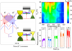 Trions are excitonic species with a positive or negative charge, and thus, unlike neutral excitons, the flow of trions can generate a net detectable charge current. Trions under favorable doping conditions can be created in a coherent manner using resonant excitation. In this work, we exploit these properties to demonstrate a gate controlled trion switch in a few-layer graphene/monolayer WS2/monolayer graphene vertical heterojunction. By using a high-resolution spectral scan through a temperature controlled variation of the band gap of the WS2 sandwich layer, we obtain a gate voltage dependent vertical photocurrent strongly relying on the spectral position of the excitation, and the photocurrent maximizes when the excitation energy is resonant with the trion peak position. Further, the resonant photocurrent thus generated can be effectively controlled by a back gate voltage applied through the incomplete screening of the bottom monolayer graphene, and the photocurrent strongly correlates with the gate dependent trion intensity, while the nonresonant photocurrent exhibits only a weak gate dependence—unambiguously proving a trion driven photocurrent generation under resonance. We estimate a sub-100 fs switching time of the device. The findings are useful towards demonstration of ultrafast excitonic devices in layered materials.
More details: Physical Review B, 101, 081413(R), 2020.
Trions are excitonic species with a positive or negative charge, and thus, unlike neutral excitons, the flow of trions can generate a net detectable charge current. Trions under favorable doping conditions can be created in a coherent manner using resonant excitation. In this work, we exploit these properties to demonstrate a gate controlled trion switch in a few-layer graphene/monolayer WS2/monolayer graphene vertical heterojunction. By using a high-resolution spectral scan through a temperature controlled variation of the band gap of the WS2 sandwich layer, we obtain a gate voltage dependent vertical photocurrent strongly relying on the spectral position of the excitation, and the photocurrent maximizes when the excitation energy is resonant with the trion peak position. Further, the resonant photocurrent thus generated can be effectively controlled by a back gate voltage applied through the incomplete screening of the bottom monolayer graphene, and the photocurrent strongly correlates with the gate dependent trion intensity, while the nonresonant photocurrent exhibits only a weak gate dependence—unambiguously proving a trion driven photocurrent generation under resonance. We estimate a sub-100 fs switching time of the device. The findings are useful towards demonstration of ultrafast excitonic devices in layered materials.
More details: Physical Review B, 101, 081413(R), 2020.
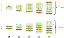 Layered transition metal dichalcogenides (TMDCs) host a variety of strongly bound exciton complexes that control the optical properties in these materials. Apart from spin and valley, layer index provides an additional degree of freedom in a few-layer-thick film. We show that in a few-layer TMDC film, the wave functions of the conduction and valence-band-edge states contributing to the K (K′) valley are spatially confined in the alternate layers––giving rise to direct (quasi-)intralayer bright exciton and lower-energy interlayer dark excitons. Depending on the spin and valley configuration, the bright-exciton state is further found to be a coherent superposition of two layer-induced states, one (E type) distributed in the even layers and the other (O type) in the odd layers. The intralayer nature of the bright exciton manifests as a relatively weak dependence of the exciton binding energy on the thickness of the few-layer film, and the binding energy is maintained up to 50 meV in the bulk limit––which is an order of magnitude higher than conventional semiconductors. Fast Stokes energy transfer from the intralayer bright state to the interlayer dark states provides a clear signature in the layer-dependent broadening of the photoluminescence peak, and plays a key role in the suppression of the photoluminescence intensity observed in TMDCs with thickness beyond a monolayer.
More details: Physical Review B, 99, 165411, 2019.
 The possibility of electrical manipulation and detection of a charged exciton (trion) before its radiative recombination makes it promising for excitonic devices. Using a few-layer graphene/monolayer WS2/monolayer graphene vertical heterojunction, we report interlayer charge transport from top few-layer graphene to bottom monolayer graphene, mediated by a coherently formed trion state. This is achieved by using a resonant excitation and varying the sample temperature; the resulting change in the WS2 bandgap allows us to scan the excitation around the exciton–trion spectral overlap with high spectral resolution. By correlating the vertical photocurrent and in situ photoluminescence features at the heterojunction as a function of the spectral position of the excitation, we show that (1) trions are anomalously stable at the junction even up to 463 K due to enhanced doping, and (2) the photocurrent results from the ultrafast formation of a trion through exciton–trion coherent coupling, followed by its fast interlayer transport. The demonstration of coherent formation, high stabilization, vertical transportation, and electrical detection of trions marks a step toward room-temperature trionics.
More details: npj 2D Materials and Applications, 3, Article number 15, 2019
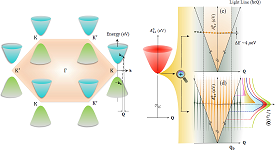 Monolayer Transition Metal Dichalcogenides (TMDS) are highly luminescent materials despite being sub-nanometer thick due to the ultra-short (<1 ps) radiative lifetime of the strongly bound bright excitons hosted by these materials. The intrinsically short radiative lifetime results in a large broadening in the exciton band with a magnitude that is about two orders greater than the spread of the light cone itself. The situation calls for a need to revisit the conventional light cone picture. We present a modified light cone concept which places the light line (ℏcQ) as the generalized lower bound for allowed radiative recombination. A self-consistent methodology, which becomes crucial upon inclusion of large radiative broadening in the exciton band, is proposed to segregate the radiative and the non-radiative components of the homogeneous exciton linewidth. We estimate a fundamental radiative linewidth of 1.54±0.17 meV, owing purely to finite radiative lifetime in the absence of non-radiative dephasing processes. As a direct consequence of the large radiative limit, we find a surprisingly large (∼0.27 meV) linewidth broadening due to zero-point energy of acoustic phonons. This obscures the precise experimental determination of the intrinsic radiative linewidth and sets a fundamental limit on the non-radiative linewidth broadening at T=0 K.
More details: Physical Review B, 99, 085412, 2019.
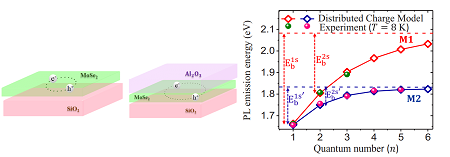 Screening due to the surrounding dielectric medium reshapes the electron-hole interaction potential and plays a pivotal role in deciding the binding energies of strongly bound exciton complexes in quantum confined monolayers of transition metal dichalcogenides (TMDs). However, owing to strong quasiparticle band-gap renormalization in such systems, a direct quantification of estimated shifts in binding energy in different dielectric media remains elusive using optical studies. By changing the dielectric environment, we show a conspicuous photoluminescence peak shift at low temperature for higher energy excitons (2s,3s,4s,5s) in monolayer MoSe2, while the 1s exciton peak position remains unaltered – a direct evidence of varying compensation between screening induced exciton binding energy modulation and quasiparticle band-gap renormalization.
More details: Physical Review B (Rapid Communication), 96, 081403(R), 2017.
 We show room-temperature valley coherence in MoS2,
MoSe2, WS2, and WSe2 monolayers using linear polarization-resolved hot photoluminescence (PL) at energies close to the excitation, demonstrating preservation of valley coherence before sufficient scattering events. The features of the copolarized hot luminescence allow us to extract the lower bound of the binding energy of the A exciton in monolayer MoS2 as 0.42 (±0.02) eV. The broadening of the PL peak is found to be dominated by a Boltzmann-type hot luminescence tail, and using the slope of the exponential decay, the carrier temperature is extracted in situ at different stages of energy relaxation. The temperature of the emitted optical phonons during the relaxation process is probed by exploiting the corresponding broadening of the Raman peaks due to temperatureinduced anharmonic effects. The findings provide a physical picture of photogeneration of valley-coherent hot carriers and their subsequent energy relaxation pathways.
We show room-temperature valley coherence in MoS2,
MoSe2, WS2, and WSe2 monolayers using linear polarization-resolved hot photoluminescence (PL) at energies close to the excitation, demonstrating preservation of valley coherence before sufficient scattering events. The features of the copolarized hot luminescence allow us to extract the lower bound of the binding energy of the A exciton in monolayer MoS2 as 0.42 (±0.02) eV. The broadening of the PL peak is found to be dominated by a Boltzmann-type hot luminescence tail, and using the slope of the exponential decay, the carrier temperature is extracted in situ at different stages of energy relaxation. The temperature of the emitted optical phonons during the relaxation process is probed by exploiting the corresponding broadening of the Raman peaks due to temperatureinduced anharmonic effects. The findings provide a physical picture of photogeneration of valley-coherent hot carriers and their subsequent energy relaxation pathways.
More details: The Journal of Physical Chemistry Letters, 7, 2032-2038, 2016.
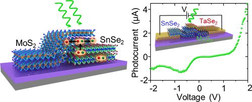 The physical proximity of layered materials in their van der Waals heterostructures (vdWhs) aids interfacial phenomena such as charge transfer (CT) and energy transfer (ET). Besides providing fundamental insights, CT and ET also offer routes to engineer optoelectronic properties of vdWhs. For example, harnessing ET in vdWhs can help to overcome the limitations of optical absorption imposed by the ultra-thin nature of layered materials and thus provide an opportunity for in situ enhancement of quantum efficiency for light-harvesting and sensing applications. While several spectroscopic studies on vdWhs probed the dynamics of CT and ET, the possible contribution of ET in the photocurrent generation remains largely unexplored. In this work, we investigate the role of nonradiative energy transfer (NRET) in the photocurrent through a vertical vdWh of SnSe2/MoS2/TaSe2. We observe an unusual negative differential photoconductance (NDPC) arising from the existence of NRET across the SnSe2/MoS2 junction. Modulation of the NRET-driven NDPC characteristics with optical power results in a striking transition of the photocurrent’s power law from a sublinear to a superlinear regime. Our observations reveal the nontrivial influence of ET on the photoresponse of vdWhs, which offer insights to harness ET in synergy with CT for vdWh based next-generation optoelectronics.
More details: ACS Nano, 15, 10, 16432–16441, 2021.
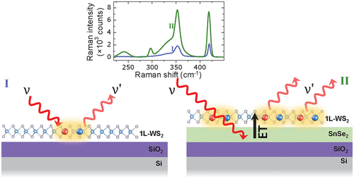 Raman enhancement techniques are essential for fundamental studies in light–matter interactions and find widespread application in microelectronics, biochemical sensing, and clinical diagnosis. Two-dimensional (2D) materials and their van der Waals heterostructures (vdWHs) are emerging rapidly as potential platforms for Raman enhancement. Here, we experimentally demonstrate a new technique of Raman enhancement driven by nonradiative energy transfer (NRET), achieving a 10-fold enhancement in the Raman intensity in a vertical vdWH comprising of a monolayer transition metal dichalcogenide (1L-TMD) placed on a multilayer SnSe2. Consequently, several weak Raman peaks become visible, which are otherwise imperceptible. We also show a strong modulation of the enhancement factor by tuning the spectral overlap between the 1L-TMD and SnSe2 through temperature variation, and the results are in remarkable agreement with a Raman polarizability model capturing the effect of NRET. The observed NRET-driven Raman enhancement is a novel mechanism that has not been experimentally demonstrated thus far and is distinct from conventional surface (SERS), tip (TERS), or interference enhanced Raman scattering (IERS) mechanisms that are driven solely by charge transfer or electric field enhancement. The mechanism can also be used in synergy with plasmonic nanostructures to achieve additional selectivity and sensitivity beyond hot spot engineering for applications like molecular detection using 2D/molecular hybrids. Our results open new avenues for engineering Raman enhancement techniques coupling the advantages of uniform enhancement accessible across a wide junction area in vertical vdWHs.
More details: ACS Photonics, 7, 2, 519–527, 2020.
Raman enhancement techniques are essential for fundamental studies in light–matter interactions and find widespread application in microelectronics, biochemical sensing, and clinical diagnosis. Two-dimensional (2D) materials and their van der Waals heterostructures (vdWHs) are emerging rapidly as potential platforms for Raman enhancement. Here, we experimentally demonstrate a new technique of Raman enhancement driven by nonradiative energy transfer (NRET), achieving a 10-fold enhancement in the Raman intensity in a vertical vdWH comprising of a monolayer transition metal dichalcogenide (1L-TMD) placed on a multilayer SnSe2. Consequently, several weak Raman peaks become visible, which are otherwise imperceptible. We also show a strong modulation of the enhancement factor by tuning the spectral overlap between the 1L-TMD and SnSe2 through temperature variation, and the results are in remarkable agreement with a Raman polarizability model capturing the effect of NRET. The observed NRET-driven Raman enhancement is a novel mechanism that has not been experimentally demonstrated thus far and is distinct from conventional surface (SERS), tip (TERS), or interference enhanced Raman scattering (IERS) mechanisms that are driven solely by charge transfer or electric field enhancement. The mechanism can also be used in synergy with plasmonic nanostructures to achieve additional selectivity and sensitivity beyond hot spot engineering for applications like molecular detection using 2D/molecular hybrids. Our results open new avenues for engineering Raman enhancement techniques coupling the advantages of uniform enhancement accessible across a wide junction area in vertical vdWHs.
More details: ACS Photonics, 7, 2, 519–527, 2020.
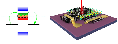
 The defect states in atomically thin layers of transition metal dichalcogenides are promising candidates for single photon emission. However, the brightness of such quantum emission is often weak and is accompanied by undesirable effects such as spectral diffusion and strong background emission. By placing a monolayer WSe2 directly on a rough gold substrate, here, we show a selective enhancement of sharp defect-bound exciton peaks, coupled with a suppressed spectral diffusion and strong quenching of background luminescence. By combining the experimental data with detailed electromagnetic simulations, we reveal that such selective luminescence enhancement originates from a combination of the Purcell effect and a wavelength dependent increment of the excitation electric field at the tips of tall rough features, coupled with a localized strain-induced exciton funneling effect. Notably, insertion of a thin hexagonal boron nitride sandwich layer between WSe2 and the Au film results in a strong enhancement of the background luminescence, obscuring the sharp defect peaks. The findings demonstrate a simple strategy of using monolayer WSe2 supported by a patterned metal film that offers a possibility of achieving quantum light sources with high purity, high brightness, and suppressed spectral diffusion.
More details: Journal of Applied Physics, 127, 073105, 2020.
The defect states in atomically thin layers of transition metal dichalcogenides are promising candidates for single photon emission. However, the brightness of such quantum emission is often weak and is accompanied by undesirable effects such as spectral diffusion and strong background emission. By placing a monolayer WSe2 directly on a rough gold substrate, here, we show a selective enhancement of sharp defect-bound exciton peaks, coupled with a suppressed spectral diffusion and strong quenching of background luminescence. By combining the experimental data with detailed electromagnetic simulations, we reveal that such selective luminescence enhancement originates from a combination of the Purcell effect and a wavelength dependent increment of the excitation electric field at the tips of tall rough features, coupled with a localized strain-induced exciton funneling effect. Notably, insertion of a thin hexagonal boron nitride sandwich layer between WSe2 and the Au film results in a strong enhancement of the background luminescence, obscuring the sharp defect peaks. The findings demonstrate a simple strategy of using monolayer WSe2 supported by a patterned metal film that offers a possibility of achieving quantum light sources with high purity, high brightness, and suppressed spectral diffusion.
More details: Journal of Applied Physics, 127, 073105, 2020.
 Graphene, owing to its zero bandgap electronic structure, is promising as an absorption material for ultra-wideband photodetection applications. However, graphene-absorption based detectors inherently suffer from poor responsivity due to weak absorption and fast photocarrier recombination, limiting their viability for low intensity light detection. Here we use a graphene/WS2/MoS2 vertical heterojunction to demonstrate a highly sensitive photodetector, where the graphene layer serves dual purpose, namely as the light absorption layer, and also as the carrier conduction channel, thus maintaining the broadband nature of the photodetector. A fraction of the photoelectrons in graphene encounter ultra-fast inter-layer transfer to a floating monolayer MoS2 quantum well providing strong quantum confined photogating effect. The photodetector shows a responsivity of 4.4 × 10⁶ A/W at 30 fW incident power, outperforming photodetectors reported till date where graphene is used as light absorption material by several orders. In addition, the proposed photodetector exhibits an extremely low noise equivalent power (NEP) of <4 fW/√Hz and a fast response (∼ milliseconds) with zero reminiscent photocurrent. The findings are attractive towards the demonstration of graphene-based highly sensitive, fast, broadband photodetection technology.
More details: ACS Applied Materials & Interfaces, 11, 30010, 2019.
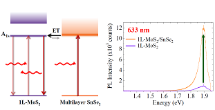 The strong light–matter interaction in monolayer transition metal dichalcogenides (TMDs) is promising for nanoscale optoelectronics with their direct band gap nature and the ultrafast radiative decay of the strongly bound excitons these materials host. However, the impeded amount of light absorption imposed by the ultrathin nature of the monolayers impairs their viability in photonic applications. Using a layered heterostructure of a monolayer TMD stacked on top of strongly absorbing, nonluminescent, multilayer SnSe2, we show that both single-photon and two-photon luminescence from the TMD monolayer can be enhanced by a factor of 14 and 7.5, respectively. This is enabled through interlayer dipole–dipole coupling induced nonradiative Förster resonance energy transfer (FRET) from SnSe2 underneath, which acts as a scavenger of the light unabsorbed by the monolayer TMD. The design strategy exploits the near-resonance between the direct energy gap of SnSe2 and the excitonic gap of monolayer TMD, the smallest possible separation between donor and acceptor facilitated by van der Waals heterojunction, and the in-plane orientation of dipoles in these layered materials. The FRET-driven uniform single- and two-photon luminescence enhancement over the entire junction area is advantageous over the local enhancement in quantum dot or plasmonic structure integrated 2D layers and is promising for improving quantum efficiency in imaging, optoelectronic, and photonic applications.
More details: ACS Nano, 13, 4795, 2019.
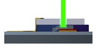
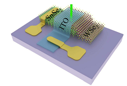 2-D transition metal di-chalcogenides are the promising candidates for ultralow intensity photodetection. However, the performance of these photodetectors is usually limited by ambience induced rapid performance degradation and long-lived charge trapping induced slow response with a large persistent photocurrent when the light source is switched off. Here, we demonstrate an indium tin oxide (ITO)/WSe2/SnSe2-based vertical double heterojunction photoconductive device where the photoexcited hole is confined in the double barrier quantum well, whereas the photo-excited electron can be transferred to either the ITO or the SnSe2 layer in a controlled manner. The intrinsically short transit time of the photoelectrons in the vertical double heterojunction helps us to achieve high responsivity in excess of 1100 A/W and fast transient response time on the order of 10 µs. A large built-in field in the WSe2 sandwich layer results in photodetection at zero external bias allowing a self-powered operation mode. The encapsulation from the top and bottom protects the photo-activeWSe2 layer from ambience induceddetrimental effects and substrate induced trapping effects helping us to achieve repeatable characteristics over many cycles.
More details: IEEE Transactions on Electron Devices, Special Issue on 2D Materials for Electronic, Optoelectronic and Sensor Devices, 65, 4141, 2018.
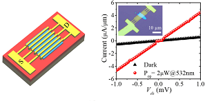 High gain photoconductive devices find wide spread applications in low intensity light detection. Ultra-thin layered materials have recently drawn a lot of attention from researchers in this regard. However, in general, a large operating voltage is required to obtain large responsivity in these devices. In addition, the characteristics are often confounded by substrate induced trap effects. We study multi-layer SnSe2 based photoconductive devices using two different structures: (1) SiO2 substrate supported inter-digitated electrode (IDE), and (2) suspended channel. The IDE device exhibits a superior low voltage performance over existing literature on planar 2D structures. However, the responsivity reduces by more than two orders of magnitude, while the transient response improves for the suspended device—providing insights into the critical role played by the channel-substrate interface in the gain mechanism. The results, on one hand, are promising for highly sensitive photoconductive applications consuming ultra-low power, and on the other hand, show a generic methodology that could be applied to other layered material based photoconductive devices as well for extracting the intrinsic behavior.
More details: Nanotechnology, 29, 035205, 2018.
 Strong light absorption, coupled with moderate carrier transport properties, makes 2D layered transition metal dichalcogenide semiconductors prom-ising candidates for low intensity photodetection applications. However, the performance of these devices is severely bottlenecked by slow response with persistent photocurrent due to long lived charge trapping, and nonreliable characteristics due to undesirable ambience and substrate effects. Here ultrahigh specific detectivity (D*) of 3.2 × 10¹⁴ Jones and responsivity (R) of 5.77 × 10⁴ A W-1 are demonstrated at an optical power density (Pop) of 0.26 W m-2 and external bias (Vext) of −0.5 V in an indium tin oxide/MoS2/copper oxide/Au vertical multi-heterojunction photodetector exhibiting small carrier transit time. The active MoS2 layer being encapsulated by carrier collection layers allows us to achieve repeatable characteristics over large number of cycles with negligible trap assisted persistent photocurrent. A large D* > 1014 Jones at zero external bias is also achieved due to the built-in field of the asymmetric photodetector.
More details: Small, 14, 1702066, 2018.
 MoS2 monolayers exhibit excellent light absorption and large thermoelectric power, which are, however, accompanied by a very strong exciton binding energy – resulting in complex photoresponse characteristics. We study the electrical response to scanning photo-excitation on MoS2 monolayer (1L) and bilayer (2L) devices, and also on monolayer/bilayer (1L/2L) planar heterojunction and monolayer/few-layer/multilayer (1L/FL/ML) planar double heterojunction devices to unveil the intrinsic mechanisms responsible for photocurrent generation in these materials and junctions. A strong photoresponse modulation is obtained by scanning the position of the laser spot, as a consequence of controlling the relative dominance of a number of layer dependent properties, including (i) the photoelectric effect (PE), (ii) the photothermoelectric effect (PTE), (iii) the excitonic effect, (iv) hot photo-electron injection from metal, and (v) carrier recombination. The monolayer and bilayer devices show a peak photoresponse when the laser is focused at the source junction, while the peak position shifts to the monolayer/few-layer junction in the heterostructure devices. The photoresponse is found to be dependent on the incoming light polarization when the source junction is illuminated, although the polarization sensitivity drastically reduces at the monolayer/few-layer heterojunction. Finally, we investigate the laser position dependent transient response of the photocurrent to reveal that trapping of carriers in SiO2 at the source junction is a critical factor to determine the transient response in 2D photodetectors, and also show that, by a systematic device design, such trapping can be avoided in the heterojunction devices, resulting in a fast transient response. The insights obtained will play an important role in designing a fast 2D TMD based photodetector and related optoelectronic and thermoelectric devices.
More details: Nanoscale, 8, 15213-15222, 2016.
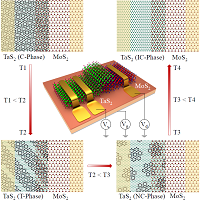
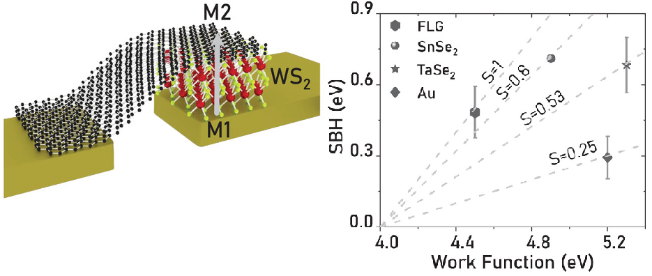 Due to Fermi level pinning (FLP), metal‐semiconductor contact interfaces result in a Schottky barrier height (SBH), which is usually difficult to tune. This makes it challenging to efficiently inject both electrons and holes using the same metal—an essential requirement for several applications, including light‐emitting devices and complementary logic. Interestingly, modulating the SBH in the Schottky–Mott limit of de‐pinned van der Waals (vdW) contacts becomes possible. However, accurate extraction of the SBH is essential to exploit such contacts to their full potential. In this study a simple technique is proposed to accurately estimate the SBH at the vdW contact interfaces by circumventing several ambiguities associated with SBH extraction. Using this technique on several vdW contacts, including metallic 2H‐TaSe2, semi‐metallic graphene, and degenerately doped semiconducting SnSe2, it is demonstrated that vdW contacts exhibit a universal de‐pinned nature. Superior ambipolar carrier injection properties of vdW contacts are demonstrated (with Au contact as a reference) in two applications, namely, a) pulsed electroluminescence from monolayer WS2 using few‐layer graphene (FLG) contact, and b) efficient carrier injection to WS2 and WSe2 channels in both n‐type and p‐type field effect transistor modes using 2H‐TaSe2 contact.
More details: Advanced Functionl Materials, 2010513, 2021.
Due to Fermi level pinning (FLP), metal‐semiconductor contact interfaces result in a Schottky barrier height (SBH), which is usually difficult to tune. This makes it challenging to efficiently inject both electrons and holes using the same metal—an essential requirement for several applications, including light‐emitting devices and complementary logic. Interestingly, modulating the SBH in the Schottky–Mott limit of de‐pinned van der Waals (vdW) contacts becomes possible. However, accurate extraction of the SBH is essential to exploit such contacts to their full potential. In this study a simple technique is proposed to accurately estimate the SBH at the vdW contact interfaces by circumventing several ambiguities associated with SBH extraction. Using this technique on several vdW contacts, including metallic 2H‐TaSe2, semi‐metallic graphene, and degenerately doped semiconducting SnSe2, it is demonstrated that vdW contacts exhibit a universal de‐pinned nature. Superior ambipolar carrier injection properties of vdW contacts are demonstrated (with Au contact as a reference) in two applications, namely, a) pulsed electroluminescence from monolayer WS2 using few‐layer graphene (FLG) contact, and b) efficient carrier injection to WS2 and WSe2 channels in both n‐type and p‐type field effect transistor modes using 2H‐TaSe2 contact.
More details: Advanced Functionl Materials, 2010513, 2021.
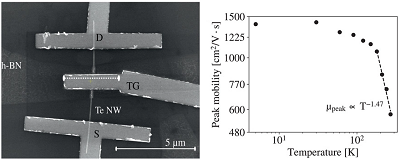 The gate‐all‐around nanowire transistor, due to its extremely tight electrostatic control and vertical integration capability, is a highly promising candidate for sub‐5 nm technology nodes. In particular, the junctionless nanowire transistors are highly scalable with reduced variability due to avoidance of steep source/drain junction formation by ion implantation. Here a dual‐gated junctionless nanowire p‐type field effect transistor is demonstrated using tellurium nanowire as the channel. The dangling‐bond‐free surface due to the unique helical crystal structure of the nanowire, coupled with an integration of dangling‐bond‐free, high quality hBN gate dielectric, allows for a phonon‐limited field effect hole mobility of 570 cm2 V−1 s−1 at 270 K, which is well above state‐of‐the‐art strained Si hole mobility. By lowering the temperature, the mobility increases to 1390 cm2 V−1 s−1 and becomes primarily limited by Coulomb scattering. The combination of an electron affinity of ≈4 eV and a small bandgap of tellurium provides zero Schottky barrier height for hole injection at the metal‐contact interface, which is remarkable for reduction of contact resistance in a highly scaled transistor. Exploiting these properties, coupled with the dual‐gated operation, we achieve a high drive current of 216 μA μm−1 while maintaining an on‐off ratio in excess of 2 × 10⁴. The findings have intriguing prospects for alternate channel material based next‐generation electronics.
More details: Advanced Functionl Materials, 2006278, 2021.
The gate‐all‐around nanowire transistor, due to its extremely tight electrostatic control and vertical integration capability, is a highly promising candidate for sub‐5 nm technology nodes. In particular, the junctionless nanowire transistors are highly scalable with reduced variability due to avoidance of steep source/drain junction formation by ion implantation. Here a dual‐gated junctionless nanowire p‐type field effect transistor is demonstrated using tellurium nanowire as the channel. The dangling‐bond‐free surface due to the unique helical crystal structure of the nanowire, coupled with an integration of dangling‐bond‐free, high quality hBN gate dielectric, allows for a phonon‐limited field effect hole mobility of 570 cm2 V−1 s−1 at 270 K, which is well above state‐of‐the‐art strained Si hole mobility. By lowering the temperature, the mobility increases to 1390 cm2 V−1 s−1 and becomes primarily limited by Coulomb scattering. The combination of an electron affinity of ≈4 eV and a small bandgap of tellurium provides zero Schottky barrier height for hole injection at the metal‐contact interface, which is remarkable for reduction of contact resistance in a highly scaled transistor. Exploiting these properties, coupled with the dual‐gated operation, we achieve a high drive current of 216 μA μm−1 while maintaining an on‐off ratio in excess of 2 × 10⁴. The findings have intriguing prospects for alternate channel material based next‐generation electronics.
More details: Advanced Functionl Materials, 2006278, 2021.
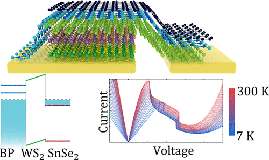 van der Waals (vdW) tunnel junctions are attractive because of their atomically sharp interface, gate tunability, and robustness against lattice mismatch between the successive layers. However, the negative differential resistance (NDR) demonstrated in this class of tunnel diodes often exhibits noisy behavior with low peak current density and lacks robustness and repeatability, limiting their practical circuit applications. Here, we propose a strategy of using a 1L-WS2 as an optimum tunnel barrier sandwiched in a broken gap tunnel junction of highly doped black phosphorus (BP) and SnSe2. We achieve high yield tunnel diodes exhibiting highly repeatable, ultraclean, and gate-tunable NDR characteristics with a signature of intrinsic oscillation, and a large peak-to-valley current ratio (PVCR) of 3.6 at 300 K (4.6 at 7 K), making them suitable for practical applications. We show that the thermodynamic stability of the vdW tunnel diode circuit can be tuned from astability to bistability by altering the constraint through choosing a voltage or a current bias, respectively. In the astable mode under voltage bias, we demonstrate a compact, voltage-controlled oscillator without the need for an external tank circuit. In the bistable mode under current bias, we demonstrate a highly scalable, single-element, one-bit memory cell that is promising for dense random access memory applications in memory intensive computation architectures.
More details: ACS Nano, 14, 11, 15678–15687, 2020.
van der Waals (vdW) tunnel junctions are attractive because of their atomically sharp interface, gate tunability, and robustness against lattice mismatch between the successive layers. However, the negative differential resistance (NDR) demonstrated in this class of tunnel diodes often exhibits noisy behavior with low peak current density and lacks robustness and repeatability, limiting their practical circuit applications. Here, we propose a strategy of using a 1L-WS2 as an optimum tunnel barrier sandwiched in a broken gap tunnel junction of highly doped black phosphorus (BP) and SnSe2. We achieve high yield tunnel diodes exhibiting highly repeatable, ultraclean, and gate-tunable NDR characteristics with a signature of intrinsic oscillation, and a large peak-to-valley current ratio (PVCR) of 3.6 at 300 K (4.6 at 7 K), making them suitable for practical applications. We show that the thermodynamic stability of the vdW tunnel diode circuit can be tuned from astability to bistability by altering the constraint through choosing a voltage or a current bias, respectively. In the astable mode under voltage bias, we demonstrate a compact, voltage-controlled oscillator without the need for an external tank circuit. In the bistable mode under current bias, we demonstrate a highly scalable, single-element, one-bit memory cell that is promising for dense random access memory applications in memory intensive computation architectures.
More details: ACS Nano, 14, 11, 15678–15687, 2020.
 Metal-based electronics is attractive for fast and radiation-hard electronic circuits and remains one of the long-standing goals for researchers. The emergence of 1T-TaS2, a layered material exhibiting strong charge density wave (CDW)-driven resistivity switching that can be controlled by an external stimulus such as electric field and optical pulses, has triggered a renewed interest in metal-based electronics. Here we demonstrate a negative differential resistor (NDR) using electrically driven CDW phase transition in an asymmetrically designed T-junction made up of 1T-TaS2/2H-MoS2 van der Waals heterojunction. The principle of operation of the proposed device is governed by majority carrier transport and is distinct from usual NDR devices employing tunneling of carriers; thus it avoids the bottleneck of weak tunneling efficiency in van der Waals heterojunctions. Consequently, we achieve a peak current density in excess of 105 nA μm-2, which is about 2 orders of magnitude higher than that obtained in typical layered material based NDR implementations. The peak current density can be effectively tuned by an external gate voltage as well as photogating. The device is robust against ambiance-induced degradation, and the characteristics repeat in multiple measurements over a period of more than a month. The findings are attractive for the implementation of active metal-based functional circuits.
More details: ACS Nano, 14, 6, 6803–6811, 2020.
Metal-based electronics is attractive for fast and radiation-hard electronic circuits and remains one of the long-standing goals for researchers. The emergence of 1T-TaS2, a layered material exhibiting strong charge density wave (CDW)-driven resistivity switching that can be controlled by an external stimulus such as electric field and optical pulses, has triggered a renewed interest in metal-based electronics. Here we demonstrate a negative differential resistor (NDR) using electrically driven CDW phase transition in an asymmetrically designed T-junction made up of 1T-TaS2/2H-MoS2 van der Waals heterojunction. The principle of operation of the proposed device is governed by majority carrier transport and is distinct from usual NDR devices employing tunneling of carriers; thus it avoids the bottleneck of weak tunneling efficiency in van der Waals heterojunctions. Consequently, we achieve a peak current density in excess of 105 nA μm-2, which is about 2 orders of magnitude higher than that obtained in typical layered material based NDR implementations. The peak current density can be effectively tuned by an external gate voltage as well as photogating. The device is robust against ambiance-induced degradation, and the characteristics repeat in multiple measurements over a period of more than a month. The findings are attractive for the implementation of active metal-based functional circuits.
More details: ACS Nano, 14, 6, 6803–6811, 2020.
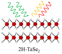 Conventional metals, in general, do not exhibit strong photoluminescence. 2H-TaSe2 is a layered transition metal dichalcogenide that possesses metallic property with charge density wave characteristics. Here we show that 2H-TaSe2 exhibits a surprisingly strong optical absorption and photoluminescence resulting from inter-band transitions. We use this perfect combination of electrical and optical properties in several optoelectronic applications. We show a sevenfold enhancement in the photoluminescence intensity of otherwise weakly luminescent multi-layer MoS2 through non-radiative resonant energy transfer from TaSe2 transition dipoles. Using a combination of scanning photocurrent and time-resolved photoluminescence measurements, we also show that the hot electrons generated by light absorption in TaSe2 have a rather long lifetime unlike conventional metals, making TaSe2 an excellent hot electron injector. Finally, we show a vertical TaSe2/MoS2/graphene photodetector demonstrating a responsivity of >10 AW-1 at 0.1 MHz—one of the fastest reported photodetectors using MoS2.
More details: Communications Physics, 2, Article number 88, 2019.
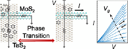
 1T-TaS2 is a layered material that exhibits charge density wave (CDW) -induced distinct electrical resistivity phases and has attracted a lot of attention for interesting device applications. However, such resistivity switching effects are often weak, and cannot be modulated by an external gate voltage — limiting their widespread usage. Using a back-gated 1T-TaS2/2H-MoS2 heterojunction, we show that the usual resistivity switching in TaS2 due to different phase transitions is accompanied with a surprisingly strong modulation in the Schottky barrier height (SBH) at the TaS2/MoS2 interface—providing an additional knob to control the degree of the phase-transition-driven resistivity switching by an external gate voltage. In particular, the commensurate (C) to triclinic (T) phase transition results in an increase in the SBH owing to a collapse of the Mott gap in TaS2. The change in SBH allows us to estimate an electrical Mott gap opening of approximately 71±7 meV in the C phase of TaS2. On the other hand, the nearly commensurate (NC) to incommensurate (IC) phase transition results in a suppression in the SBH, and the heterojunction shows a gate-controlled resistivity switching ratio up to 17.3, which is approximately 14.5 times higher than that of stand-alone TaS2. The findings mark an important step forward showing a promising pathway to externally control as well as amplify the CDW-induced resistivity switching. This will boost device applications that exploit these phase transitions, such as ultra-broadband photodetection, negative differential conductance, fast oscillator and threshold switching in neuromorphic circuits.
More details: Physical Review Applied, 11, 024031, 2019.
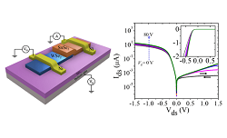 Backward diodes conduct more efficiently in the reverse bias than in the forward bias, providing superior high-frequency response, temperature stability, radiation hardness, and 1/f noise performance than a conventional diode conducting in the forward direction. We demonstrate a van der Waals material-based backward diode by exploiting the giant staggered band offsets of WSe2/SnSe2 vertical heterojunction. The diode exhibits an ultrahigh-reverse rectification ratio (R) of ∼2.1 × 10⁴, and the same is maintained up to an unusually large bias of 1.5 V outperforming existing backward diode reports using conventional bulk semiconductors as well as one- and two-dimensional materials by more than an order of magnitude while maintaining an impressive curvature coefficient (γ) of ∼37 V-1. The transport mechanism in the diode is shown to be efficiently tunable by external gate and drain bias, as well as by the thickness of the WSe2 layer and the type of metal contacts used. These results pave the way for practical electronic circuit applications using two-dimensional materials and their heterojunctions.
More details: ACS Applied Materials & Interfaces, 10, 5657, 2018.
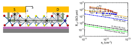 Monolayers of transition metal dichalcogenides (TMDCs) exhibit excellent electronic and optical properties. However, the performance of these two-dimensional (2D) devices are often limited by the large resistance offered by the metal contact interface. To date, the carrier injection mechanism from metal to 2D TMDC layers remains unclear, with widely varying reports of Schottky barrier height (SBH) and contact resistance (Rc), particularly in the monolayer limit. We use a combination of theory and experiments in Au and Ni contacted monolayer MoS2 device to elucidate the following points: (i) the carriers are injected at the source contact through a cascade of two potential barriers—the barrier heights being determined by the degree of interaction between the metal and the TMDC layer; (ii) the conventional Richardson equation becomes invalid due to the multidimensional nature of the injection barriers, and using Bardeen-Tersoff theory, we derive the appropriate form of the Richardson equation that describes such a composite barrier; (iii) we propose a novel transfer length method (TLM) based SBH extraction methodology, to reliably extract SBH by eliminating any confounding effect of temperature dependent channel resistance variation; (iv) we derive the Landauer limit of the contact resistance achievable in such devices. A comparison of the limits with the experimentally achieved contact resistance reveals plenty of room for technological improvements.
More details: Physical Review B, 96, 205423, 2017.
 We revisit the theory of negative capacitance in: 1) a standalone ferroelectric; 2) a ferroelectric dielectric; and 3) a ferroelectric–semiconductor series combination, and show that it is important to minimize the total Gibbs free energy of the combined system (and not just the free energy of the ferroelectric) to obtain the correct states. The theory is explained both analytically and using numerical simulation, for ferroelectric materials with the first-order and second-order phase transitions. The exact conditions for different regimes of operation in terms of hysteresis and gain are derived for ferroelectric–dielectric combination. Finally, the ferroelectric semiconductor series combination is analyzed to gain insights into the possibility of realization of steep slope transistors in a hysteresis-free manner.
More details: IEEE Transactions on Electron Devices, Vol. 63, No. 5, pp. 2043-2049, 2016.